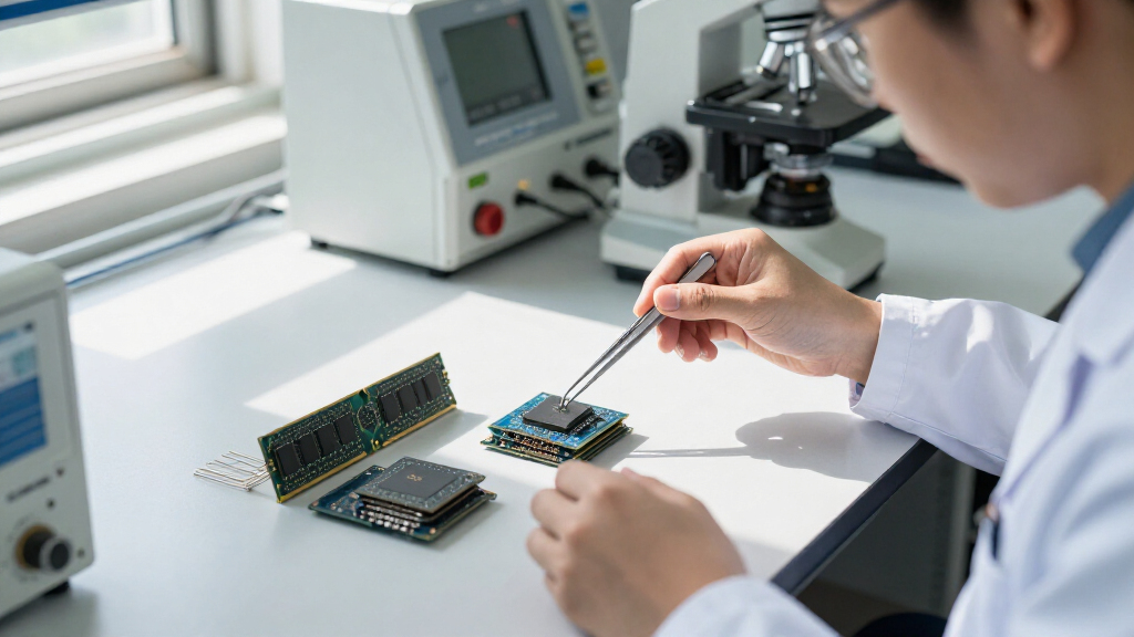
🔍 Read the full analysis: A Closer Look At AI Chip Dies, Memory Stacks And Packaging on ThorstenMeyerAI.com

Prime made for students and young adults
- Fast, free delivery for dorm and study essentials
- Prime Video and Amazon Music included
- Member-only deals
TL;DR
A Nov. 22 explainer from ThorstenMeyerAI.com maps AI accelerators from compute dies and stacked high-bandwidth memory to the interposer, cooling system and rack. Its central point is that performance and deployment depend not only on compute chips, but also on memory bandwidth, advanced packaging capacity and available supply.
ThorstenMeyerAI.com published a hardware explainer on November 22 showing how modern AI accelerators combine compute dies, stacked high-bandwidth memory (HBM), silicon interposers and cooling hardware—and how those packages fit into large server racks. The report argues that memory bandwidth and advanced packaging capacity, not just the number of compute chips, help determine accelerator performance and how many systems manufacturers can supply.
The explainer uses schematic 3D models to show a package from the bottom up: a package substrate carries power and signals; a silicon interposer links the compute dies and memory; and liquid cooling hardware sits above the chips. The author says the models preserve layer order and component counts but use schematic dimensions. Nvidia and AMD do not publish the dimensions needed to establish the parts’ exact sizes, the report says.
On the memory side, HBM consists of DRAM chips stacked vertically and connected through-silicon vias, or TSVs. That arrangement places memory close to the processor and allows many connections in a compact area. The source cites Nvidia’s product information for a rise in stated bandwidth from 900 GB/s for V100 to 19.2 TB/s for Rubin. Those figures describe the products named; they do not, on their own, establish how a particular workload will perform.
The report also compares current accelerator designs. It says Nvidia’s Rubin GPU uses two reticle-limited compute dies, while AMD’s MI355X combines eight stacked accelerator complex dies and two I/O dies with eight 12-high memory stacks. These details are attributed to the companies’ product and architecture materials. The report says a silicon interposer, including packaging made through TSMC’s CoWoS technologies, provides the dense wiring needed to connect the components.
Why Memory and Packaging Constrain AI
The package-level view matters because an AI accelerator is not simply one large processor. Its compute dies need data delivered quickly, and the memory system and connections between components can limit how effectively that compute is used. HBM’s proximity and bandwidth are central to feeding the processor, while interposers let manufacturers connect many dies and memory stacks with far more wiring than a conventional circuit board can provide.
Packaging also affects supply. TSMC’s CoWoS processes assemble large, complex packages, and the source describes that step as a production bottleneck in its own right. Even if compute dies are available, constrained capacity for advanced packaging or HBM can limit the number of complete accelerators. For businesses planning AI infrastructure, that can shape availability, deployment schedules and costs; the report does not provide a market price or quantify those effects.
At rack scale, the requirements extend beyond chips. The source says Nvidia GB200 and GB300 NVL72 systems pair 72 GPUs with 36 CPUs, along with switch trays, power shelves and liquid cooling. A rack’s useful capacity therefore depends on coordinated supplies of processors, memory, packaging, networking, power and cooling—not a GPU count alone.
Products Worth Considering

Bose TV Speaker Compact Soundbar with Bluetooth and HDMI-ARC, Black

Amazon Kindle Paperwhite (2024), 16 GB, 7-inch Display, Black

LG UltraGear 34G600A-B 34-Inch Curved WQHD Gaming Monitor
As an affiliate, we earn on qualifying purchases.
From Silicon Layers to Full Racks
The report places the designs in a short hardware timeline. Nvidia’s Blackwell Ultra is described as having two reticle-sized dies joined by a die-to-die link, while the Rubin architecture uses two reticle-limited compute dies. AMD’s MI350 Series takes a more vertically integrated approach, stacking eight accelerator complex dies over two I/O dies; the report identifies the MI355X as a 185-billion-transistor product. AMD’s next-generation MI450X and MI455X are described by the company as using stacked 3D hybrid-bonded compute dies.
A reticle is the maximum area a lithography scanner can print in one exposure. According to the source’s account of TSMC information, CoWoS-S accommodates an interposer up to about 2,700 square millimeters, while CoWoS-L uses silicon bridges in a carrier to support larger designs. The report says TSMC’s CEO described five-reticle-size production as operating in the real world on October 15, 2026, and said the company was working toward larger formats. These are attributed company statements, not independent measures of production capacity.
The rack examples show the scale of integration. The article cites Nvidia documentation for 18 compute trays and nine NVLink switch trays in an NVL72 rack, plus management switches and power shelves. Nvidia’s cited documentation gives a 120-kilowatt cooling capacity for a GB200 NVL72 rack. The author notes that the models’ sizes are schematic, so they should be read as illustrations of layer arrangement and counts rather than dimensional engineering drawings.
“Demand [is expected] to exceed supply “through 2030.””
— SK hynix, as quoted in the ThorstenMeyerAI.com explainer
What the Models Cannot Establish
The explainer is a technical overview, not a teardown or independent production audit. Its models use schematic dimensions, and the article says exact die, package and memory-stack measurements are not publicly available from Nvidia or AMD. The illustrations therefore cannot confirm physical proportions, manufacturing yields or the precise construction of every vendor’s product.
Several performance and supply statements come from company materials. The cited bandwidth figures are product specifications, not a direct comparison of application speed. SK hynix’s expectation that demand will exceed supply through 2030 is a company forecast; the report does not define the size of the expected gap or how it could change. It also does not establish how much packaging capacity each accelerator generation will receive or how those constraints will affect prices.
The source identifies a current Vera Rubin NVL72 listing as “Available Now,” but does not provide independent confirmation of availability by region, shipment volume or customer access. Those details remain unclear from the material provided.
Track Supply and Rack Availability
The next useful indicators are vendor shipment and availability updates, HBM production guidance and disclosures about advanced packaging capacity. Those measures would help show whether manufacturers can deliver complete systems at the scale implied by their product specifications. The source does not identify a scheduled follow-up announcement or a specific date for a new supply update.
For buyers, the practical questions are whether accelerator racks can be obtained on the required schedule, what configurations are offered, and whether facilities can support their power and liquid-cooling needs. The explainer lays out the hardware dependencies, but it does not give delivery timelines, pricing or customer allocation figures. Those remain important open points as AI infrastructure plans move from specifications to deployment.
Key Questions
What is an AI accelerator package made of?
In the report’s examples, a package combines compute dies, HBM stacks and a silicon interposer on a package substrate. Cooling hardware is installed above the chips in the server system.
What does HBM do?
HBM is DRAM arranged in vertical stacks and connected by through-silicon vias. Its placement close to the compute dies provides high-bandwidth access to memory, which helps supply data to the processor.
Why does packaging affect AI chip supply?
Advanced packaging connects multiple dies and memory stacks into a working unit. If packaging capacity is limited, manufacturers may not be able to turn available components into complete accelerators at the desired rate.
How many GPUs are in an Nvidia NVL72 rack?
The source describes GB200 and GB300 NVL72 racks as containing 72 GPUs and 36 CPUs, alongside networking, power and cooling equipment. The configuration cited is not a guarantee of current availability.
Are the article’s 3D models to scale?
No. The explainer says its models show layer order and component counts but use schematic sizes because exact dimensions are not published in the cited materials.
Source: ThorstenMeyerAI.com